|
我的QQ:282965382 邮箱nicebuidlings@gmail.com 希望高手指教 如果我问题没说清的话 需要什么资料我可以通过邮箱发过去,谢谢 |
|
各位大大们,我最近做毕业设计,需要在硬件上演示,用的是Cyclone III starter board 说实话,我现在都不是很懂这些东西,不知道能不能讲清,我的情况是这样的 想要演示的是一个VHDL的程序,其输出是I[7..0] I_clk Q[7..0] Q_clk,也就是I,Q两路8位数字信号和对应的时钟。目的是通过DA变化把信道输出到频谱仪上把输出信号演示 用到的器材是Cyclone III starter board,THDB_ADA 现在碰到的问题是不知道怎么配置管脚,我现在有CIII_Starter_Kit的示例工程,但是看不太懂,求高手指教 |
|
“最后 TO 友晶的大大们 我觉得呢。。随着大陆这边越来越多的人选择友晶的母版及子卡。 或许更全面及亲切的入门手册及指导书是有意义的 其中,也还是考虑一下大陆这边的情况罗 : ) 可能在TaiWan,这个已经很入门了。。但是我自己也觉得。。 当初在用DE开发板及子卡的时候,还是希望能有个更入门更详细的指导书呢 : ) 谢谢了哟,嘿嘿” 好建议! |
|
本帖最后由 huguangheng 于 2010-1-11 22:13 编辑 //-------------------------------------------------------------------------------------------- 转一下我的回复, 关于ADA,因为我当初用得是3C120的开发板,所以引脚和DE2-70不一样,无法直接把代码给你看。如果希望弄清楚引脚的连接,需要参考DE2-70和ADA的datasheet,以及DE2-70的范例中的qsf里的引脚设置。从sch图中可以得到结果 关于接口。除了数据和时钟外,有低电平有效的使能信号,以及一个power_on,至于inter模式,我当初没有使用,所以不清楚引脚情况。 仔细看光盘中的内容,尤其是性能评估的那份资料,里面有信噪比的那个,你会发现有清楚地讲到这个范例是用NCO,LPM_ADD先生成信号,再由DA输出,AD采集,并分析其信号质量。(ps,这也是个联合测量AD,DA的好办法) 关于数据输出的处理。我没有仔细分析。。大概猜了下, 对于“纯正”信号:如果是我要提供待测试的数字信源,首先要避免数据溢出,考虑src和snk端的数据格式不同,比如符号位。如果考虑snk端特性(比如对于AD,希望信源幅度和频率都能在信噪比相对高的范围内),比如,在无放大的情况下,数字端就让数据处于比较合适的幅度。 对于产生“特别”的波形:比如为了产生多个频率和不同程度谐波,以及产生缓变和陡变信号,甚至毛刺和震荡之类。。(扯远了。。),可以在bus输出端里简单的调整一下特定bit,这样在定性不定量的简单测试中比做一个复杂的新源还是方便得多 不过以上我都瞎猜的,没有仔细想啊。。。 关于最后那个AD,DA,实际能工作在多少,首先,理论上是2倍信号频率的时钟就可以,即一个周期采2个点,理论上可以复原信号。但是实际中大部分时候都不会这样,相信如果你自己试过的话,就印象更深刻了。 比如说你可以使用NCO的IP,然后在配置参数时,在固定系统时钟下,即fs下,输出信号的频率从低到高,直到逼近1/2系统时钟时,输出信号的信噪会怎么变化。可以自己玩一下 : ) 那么到底,系统/采样时钟和信号的比例是多少,根据不同系统来定。你可以参考DSP原理的书,或者看ADI啊,Linear等的AD/DA设计及选型方案。或者直接看信号质量你系统中相邻的模块能不能接受罗,比如用DA输出正弦波,再用模拟filter来还原,低频下,根据信号还原的要求和滤波器制作难度,数字部分一般最少会4~10倍采样,不过模拟的人可能要有意见了,那么就可能会提高几倍,甚至数量级,如果模拟部分处理得很好,甚至数字部分本身就还有一些模块来提高信噪比,那么也有极端到2.5倍的。 //------------------------------------------------------------------- 最后 TO 友晶的大大们 我觉得呢。。随着大陆这边越来越多的人选择友晶的母版及子卡。 或许更全面及亲切的入门手册及指导书是有意义的 其中,也还是考虑一下大陆这边的情况罗 : ) 可能在TaiWan,这个已经很入门了。。但是我自己也觉得。。 当初在用DE开发板及子卡的时候,还是希望能有个更入门更详细的指导书呢 : ) 谢谢了哟,嘿嘿 |
|
***省略*** //============================================================================= // REG/WIRE declarations //============================================================================= output [13:0]a2dba; //这个信号用来干嘛?是用于信号的反馈测试吗? output [13:0]a2dbb; //这个信号用来干嘛?是用于信号的反馈测试吗? //assign a2db = {GPIO_0[14],GPIO_0[15],GPIO_0[16],GPIO_0[18],GPIO_0[17],GPIO_0[19],GPIO_0[20],GPIO_0[22], //GPIO_0[21],GPIO_0[23],GPIO_0[24],GPIO_0[26],GPIO_0[25],GPIO_0[27]}; assign a2dba = {GPIO_0[27],GPIO_0[25],GPIO_0[26],GPIO_0[24],GPIO_0[23],GPIO_0[21],GPIO_0[22],GPIO_0[20], GPIO_0[19],GPIO_0[17],GPIO_0[18],GPIO_0[16],GPIO_0[15],GPIO_0[14]}; assign a2dbb = {GPIO_0[13],GPIO_0[11],GPIO_0[12],GPIO_0[10],GPIO_0[9],GPIO_0[7],GPIO_0[8],GPIO_0[6], GPIO_0[5],GPIO_0[3],GPIO_0[4],GPIO_0[2],GPIO_0[1],GPIO_0[0]}; assign {GPIO_1[15],GPIO_1[17],GPIO_1[18],GPIO_1[20],GPIO_1[19],GPIO_1[21],GPIO_1[23],GPIO_1[25], GPIO_1[22],GPIO_1[24],GPIO_1[27],GPIO_1[29],GPIO_1[26],GPIO_1[28]} = comb; //接到DAC数据输入端口B assign {GPIO_1[0],GPIO_1[1],GPIO_1[2],GPIO_1[4],GPIO_1[3],GPIO_1[5],GPIO_1[6],GPIO_1[8], GPIO_1[7],GPIO_1[9],GPIO_1[10],GPIO_1[12],GPIO_1[11],GPIO_1[13]} = comb; //接到DAC数据输入端口A assign GPIO_1[30] = CLK_125; //Input write signal for PORT B 接到DAC的WRT1端口 assign GPIO_1[14] = CLK_125; //Input write signal for PORT A 接到DAC的WRT2端口 assign GPIO_1[31] = 1; //Mode Select. 1 = dual port, 0 = interleaved. 接到DAC的Mode assign GPIO_0[28] = 1; //POWER ON 电源有效? assign GPIO_0[29] = 0; //Enable B 这个AD9767芯片有低电平有效的使能信号吗? assign GPIO_0[31] = 0; //Enable A 这个AD9767芯片有低电平有效的使能信号吗 output CLK_100; // 这个CLK_100写的是输出端口,但是它哪里也没有接,它是用来干嘛的? wire [31:0]phasinc1; wire [31:0]phasinc2; wire g = 0; wire v = 1; assign phasinc1 = {g,g,g,g,v,v,g,g,v,v,g,g,v,v,g,g,v,v,g,g,v,v,g,g,v,v,g,g,v,v,g,v}; //用于NCO231产生振波 assign phasinc2 = {g,v,g,g,g,g,g,g,g,g,g,g,g,g,g,g,g,g,g,g,g,g,g,g,g,g,g,g,g,g,g,g}; //形数据? output [13:0]sin10_out; output [13:0]sin_out; wire sn; wire s10n; assign sn = ~sin_out[12]; assign s10n = ~sin10_out[12]; assign GPIO_CLKOUT_P1 = CLK_125; //PLL Clock to DAC_B 接到DAC的通路B的CLK? assign GPIO_CLKOUT_N1 = CLK_125; //PLL Clock to DAC_A 接到DAC通路A的CLK? assign GPIO_CLKOUT_P0 = CLK_65; //PLL Clock to ADC_B assign GPIO_CLKOUT_N0 = CLK_65; //PLL Clock to ADC_A output [13:0]comb; //============================================================================= // Structural coding //============================================================================= nco231 sin1 (.phi_inc_i(phasinc1), .clk(CLK_125), .clken(v), .reset_n(g), .fsin_o(sin_out), .out_valid(ovalid)); nco231 sin2 (.phi_inc_i(phasinc2), .clk(CLK_125), .clken(v), .reset_n(g), .fsin_o(sin10_out), .out_valid(ovalid)); pll pll_100 (.inclk0(iCLK_50), .pllena(v), .areset(g), .c0(CLK_125), .c1(CLK_65)); lpm_add lpm (.clock(CLK_125), .dataa({g,sn,sin_out[11:0]}), // 为什么sn要写成 sn = ~sin_out[12];??? .datab({g,s10n,sin10_out[11:0]}),//这个输入数据为什么最高位要取0呢? .result(comb)); //输出数据应该是14BIT的普通数据吧,有什么约束吗? //assign comb = (iSW[17]) ? (iSW[16]) ? (iSW[15]) ? {sn,sin_out[12:0]} : tri_data : ramp_data : square; endmodule 因为我是第一次用DAC,所以对它的参数理解不是很深刻,还有一个问题就是THDB_ADA子板卡上的AD9767 DAC芯片的最大采样率是125MSPS,那么它的最高工作频率是用125MSPS这个参数通过“采样公式”计算125*0.5= 62.5 MHZ?还是芯片使用手册上所写的40MHZ呢?根据我看的资料,DAC芯片的最大工作频率是由芯片的“Maximum Output Update Rate (fCLK) ”决定的,那么AD9767的 Maximum Output Update Rate (fCLK) 是125MHZ,那这是否又意味着芯片的最高工作频率是125MHZ呢?总结这个问题就是板卡上所用的AD9767的最高工作频率是多少?40MHZ?65MHZ?还是125MHZ?这个最高工作频率到底是怎么算出来的,由芯片的什么参数决定呢,这个问题搞的我都有点晕了,如果可以,也请你帮我看一下。 |
|
经同意,转一位朋友的提问和我的回复如下,希望能有朋友进一步帮忙 //------------------------------------------------------------------------------- 我现在在使用贵公司的THDB_ADA子板卡配合DE2_70开发板做一个波形发生器,通过阅读THDB_ADA的DATASHEET,我知道了子板卡上数模转换芯片AD9767的引脚接法,但是就是不知道当THDB_ADA板卡通过GPIO扩展口接到DE2_70上时,芯片AD9767的引脚和GPIO0及GPIO1接口是怎么连的,即芯片的引脚是怎么一一对应连到GPIO的引脚的,通过THDB_ADA板卡附带的那张光盘中范例,我也看不出这些脚是怎么连的,只能去猜,下面的代码是DE2_70_ADA的那个范例的顶层文件,我把我对GPIO与DAC的相互连接的语句写上注释了,你帮我看看我理解的对不对的? module DE2_70_TOP ( //////////////////// Clock Input //////////////////// iCLK_28, // 28.63636 MHz iCLK_50, // 50 MHz iCLK_50_2, // 50 MHz iCLK_50_3, // 50 MHz iCLK_50_4, // 50 MHz iEXT_CLOCK, // External Clock //////////////////// Push Button //////////////////// iKEY, // Pushbutton[3:0] //////////////////// DPDT Switch //////////////////// iSW, // Toggle Switch[17:0] //////////////////// 7-SEG Dispaly //////////////////// oHEX0_D, // Seven Segment Digit 0 oHEX0_DP, // Seven Segment Digit 0 decimal point oHEX1_D, // Seven Segment Digit 1 oHEX1_DP, // Seven Segment Digit 1 decimal point oHEX2_D, // Seven Segment Digit 2 oHEX2_DP, // Seven Segment Digit 2 decimal point oHEX3_D, // Seven Segment Digit 3 oHEX3_DP, // Seven Segment Digit 3 decimal point oHEX4_D, // Seven Segment Digit 4 oHEX4_DP, // Seven Segment Digit 4 decimal point oHEX5_D, // Seven Segment Digit 5 oHEX5_DP, // Seven Segment Digit 5 decimal point oHEX6_D, // Seven Segment Digit 6 oHEX6_DP, // Seven Segment Digit 6 decimal point oHEX7_D, // Seven Segment Digit 7 oHEX7_DP, // Seven Segment Digit 7 decimal point //////////////////////// LED //////////////////////// oLEDG, // LED Green[8:0] oLEDR, // LED Red[17:0] //////////////////////// UART //////////////////////// oUART_TXD, // UART Transmitter iUART_RXD, // UART Receiver oUART_CTS, // UART Clear To Send iUART_RTS, // UART Requst To Send //////////////////////// IRDA //////////////////////// oIRDA_TXD, // IRDA Transmitter iIRDA_RXD, // IRDA Receiver ///////////////////// SDRAM Interface //////////////// DRAM_DQ, // SDRAM Data bus 32 Bits oDRAM0_A, // SDRAM0 Address bus 13 Bits oDRAM1_A, // SDRAM1 Address bus 13 Bits oDRAM0_LDQM0, // SDRAM0 Low-byte Data Mask oDRAM1_LDQM0, // SDRAM1 Low-byte Data Mask oDRAM0_UDQM1, // SDRAM0 High-byte Data Mask oDRAM1_UDQM1, // SDRAM1 High-byte Data Mask oDRAM0_WE_N, // SDRAM0 Write Enable oDRAM1_WE_N, // SDRAM1 Write Enable oDRAM0_CAS_N, // SDRAM0 Column Address Strobe oDRAM1_CAS_N, // SDRAM1 Column Address Strobe oDRAM0_RAS_N, // SDRAM0 Row Address Strobe oDRAM1_RAS_N, // SDRAM1 Row Address Strobe oDRAM0_CS_N, // SDRAM0 Chip Select oDRAM1_CS_N, // SDRAM1 Chip Select oDRAM0_BA, // SDRAM0 Bank Address oDRAM1_BA, // SDRAM1 Bank Address oDRAM0_CLK, // SDRAM0 Clock oDRAM1_CLK, // SDRAM1 Clock oDRAM0_CKE, // SDRAM0 Clock Enable oDRAM1_CKE, // SDRAM1 Clock Enable //////////////////// Flash Interface //////////////// FLASH_DQ, // FLASH Data bus 15 Bits (0 to 14) FLASH_DQ15_AM1, // FLASH Data bus Bit 15 or Address A-1 oFLASH_A, // FLASH Address bus 26 Bits oFLASH_WE_N, // FLASH Write Enable oFLASH_RST_N, // FLASH Reset oFLASH_WP_N, // FLASH Write Protect /Programming Acceleration iFLASH_RY_N, // FLASH Ready/Busy output oFLASH_BYTE_N, // FLASH Byte/Word Mode Configuration oFLASH_OE_N, // FLASH Output Enable oFLASH_CE_N, // FLASH Chip Enable //////////////////// SRAM Interface //////////////// SRAM_DQ, // SRAM Data Bus 32 Bits SRAM_DPA, // SRAM Parity Data Bus oSRAM_A, // SRAM Address bus 22 Bits oSRAM_ADSC_N, // SRAM Controller Address Status oSRAM_ADSP_N, // SRAM Processor Address Status oSRAM_ADV_N, // SRAM Burst Address Advance oSRAM_BE_N, // SRAM Byte Write Enable oSRAM_CE1_N, // SRAM Chip Enable oSRAM_CE2, // SRAM Chip Enable oSRAM_CE3_N, // SRAM Chip Enable oSRAM_CLK, // SRAM Clock oSRAM_GW_N, // SRAM Global Write Enable oSRAM_OE_N, // SRAM Output Enable oSRAM_WE_N, // SRAM Write Enable //////////////////// ISP1362 Interface //////////////// OTG_D, // ISP1362 Data bus 16 Bits oOTG_A, // ISP1362 Address 2 Bits oOTG_CS_N, // ISP1362 Chip Select oOTG_OE_N, // ISP1362 Read oOTG_WE_N, // ISP1362 Write oOTG_RESET_N, // ISP1362 Reset OTG_FSPEED, // USB Full Speed, 0 = Enable, Z = Disable OTG_LSPEED, // USB Low Speed, 0 = Enable, Z = Disable iOTG_INT0, // ISP1362 Interrupt 0 iOTG_INT1, // ISP1362 Interrupt 1 iOTG_DREQ0, // ISP1362 DMA Request 0 iOTG_DREQ1, // ISP1362 DMA Request 1 oOTG_DACK0_N, // ISP1362 DMA Acknowledge 0 oOTG_DACK1_N, // ISP1362 DMA Acknowledge 1 //////////////////// LCD Module 16X2 //////////////// oLCD_ON, // LCD Power ON/OFF oLCD_BLON, // LCD Back Light ON/OFF oLCD_RW, // LCD Read/Write Select, 0 = Write, 1 = Read oLCD_EN, // LCD Enable oLCD_RS, // LCD Command/Data Select, 0 = Command, 1 = Data LCD_D, // LCD Data bus 8 bits //////////////////// SD_Card Interface //////////////// SD_DAT, // SD Card Data SD_DAT3, // SD Card Data 3 SD_CMD, // SD Card Command Signal oSD_CLK, // SD Card Clock //////////////////// I2C //////////////////////////// I2C_SDAT, // I2C Data oI2C_SCLK, // I2C Clock //////////////////// PS2 //////////////////////////// PS2_KBDAT, // PS2 Keyboard Data PS2_KBCLK, // PS2 Keyboard Clock PS2_MSDAT, // PS2 Mouse Data PS2_MSCLK, // PS2 Mouse Clock //////////////////// VGA //////////////////////////// oVGA_CLOCK, // VGA Clock oVGA_HS, // VGA H_SYNC oVGA_VS, // VGA V_SYNC oVGA_BLANK_N, // VGA BLANK oVGA_SYNC_N, // VGA SYNC oVGA_R, // VGA Red[9:0] oVGA_G, // VGA Green[9:0] oVGA_B, // VGA Blue[9:0] //////////// Ethernet Interface //////////////////////// ENET_D, // DM9000A DATA bus 16Bits oENET_CMD, // DM9000A Command/Data Select, 0 = Command, 1 = Data oENET_CS_N, // DM9000A Chip Select oENET_IOW_N, // DM9000A Write oENET_IOR_N, // DM9000A Read oENET_RESET_N, // DM9000A Reset iENET_INT, // DM9000A Interrupt oENET_CLK, // DM9000A Clock 25 MHz //////////////// Audio CODEC //////////////////////// AUD_ADCLRCK, // Audio CODEC ADC LR Clock iAUD_ADCDAT, // Audio CODEC ADC Data AUD_DACLRCK, // Audio CODEC DAC LR Clock oAUD_DACDAT, // Audio CODEC DAC Data AUD_BCLK, // Audio CODEC Bit-Stream Clock oAUD_XCK, // Audio CODEC Chip Clock //////////////// TV Decoder //////////////////////// iTD1_CLK27, // TV Decoder1 Line_Lock Output Clock iTD1_D, // TV Decoder1 Data bus 8 bits iTD1_HS, // TV Decoder1 H_SYNC iTD1_VS, // TV Decoder1 V_SYNC oTD1_RESET_N, // TV Decoder1 Reset iTD2_CLK27, // TV Decoder2 Line_Lock Output Clock iTD2_D, // TV Decoder2 Data bus 8 bits iTD2_HS, // TV Decoder2 H_SYNC iTD2_VS, // TV Decoder2 V_SYNC oTD2_RESET_N, // TV Decoder2 Reset //////////////////// GPIO //////////////////////////// GPIO_0, // GPIO Connection 0 I/O GPIO_CLKIN_N0, // GPIO Connection 0 Clock Input 0 GPIO_CLKIN_P0, // GPIO Connection 0 Clock Input 1 GPIO_CLKOUT_N0, // GPIO Connection 0 Clock Output 0 GPIO_CLKOUT_P0, // GPIO Connection 0 Clock Output 1 GPIO_1, // GPIO Connection 1 I/O GPIO_CLKIN_N1, // GPIO Connection 1 Clock Input 0 GPIO_CLKIN_P1, // GPIO Connection 1 Clock Input 1 GPIO_CLKOUT_N1, // GPIO Connection 1 Clock Output 0 GPIO_CLKOUT_P1 // GPIO Connection 1 Clock Output 1 ,sin_out ,sin10_out ,comb //从sin_out---CLK_100这6个信号在QSF文件中看,并没有引脚的分配, ,a2dba //为什么要写在顶层的端口列表中呢? 而不是以中间信号REG或WIRE ,a2dbb //的形式写端口列表外面呢? 这样写有什么作用? ,CLK_100 ); |
|
7# bear 我用的8.1,后来没有更换过。 |
|
本帖最后由 bear 于 2010-1-4 19:47 编辑 huguangheng ,谢谢您的回复,LPM_ADD这个IP模块我重新的添加过,去除它也试过,问题还是老样子,问题可能还是出在NCO上,在QUARTUS II9.0 的环境底下可以重新的编译PLL和LPM的IP核,但是就是找不到NCO的IP核,可能是9.0的环境不支持实例中NCO的IP核?还有,要是你看到我的留言,可否告知你是用QUARTUS的什么版本跑那个范例的?  |
|
我覺得應該是範例裡頭用的那個nco megafunction的問題,因為附的是早期版本的nco megafunction,但新版的Quartus只會安裝最新版本的nco megafunction,導致重新compile時找不到相對應的module而發生錯誤。 這種情況在我之前用Altera自己的DSP Kit時也有發生過,解決方法是自己更新並替換掉原來的nco megafunction,或是安裝舊版的nco megafuntion,反正這個範例就如同huguangheng所說的,重點是把相關的引腳都拉了出來給使用者。 至於ADA的售價 .. 老實說目前還沒有看到性價比高過它的,個人推測應該主要是卡在AD/DA IC的成本吧。 |
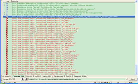
上面的图看不清楚,我把出错信息贴在这里: 错误好像和那个小LPM_ADD有关吧,是不是路劲什么的问题啊, 其实你也可以把这个去掉了,看还会不会有错,不是非要用这个模块 而且ADA的驱动因为是超级简单的那种并行,给时钟出数据的那种 所以你自己也可以理解一下那个示例工程,不需要多在意细节 其实个人觉得那个示例工程有用的地方就是把引脚告诉你了。。。 PS:话说ADA用着还是很爽的。。如果能便宜点就好了。。 |
|
2# bear 我前不久用过的。。。当时一切正常。。。。 |
|
上面的图看不清楚,我把出错信息贴在这里: Info: Elaborated megafunction instantiation "pll:pll_100|altpll:altpll_component" Info: Instantiated megafunction "pll:pll_100|altpll:altpll_component" with the following parameter: Info: Parameter "clk0_divide_by" = "2" Info: Parameter "clk0_duty_cycle" = "50" Info: Parameter "clk0_multiply_by" = "5" Info: Parameter "clk0_phase_shift" = "0" Info: Parameter "clk1_divide_by" = "4" Info: Parameter "clk1_duty_cycle" = "50" Info: Parameter "clk1_multiply_by" = "5" Info: Parameter "clk1_phase_shift" = "0" Info: Parameter "compensate_clock" = "CLK0" Info: Parameter "gate_lock_signal" = "NO" Info: Parameter "inclk0_input_frequency" = "20000" Info: Parameter "intended_device_family" = "Cyclone II" Info: Parameter "invalid_lock_multiplier" = "5" Info: Parameter "lpm_hint" = "CBX_MODULE_PREFIX=pll" Info: Parameter "lpm_type" = "altpll" Info: Parameter "operation_mode" = "NORMAL" Info: Parameter "port_activeclock" = "PORT_UNUSED" Info: Parameter "port_areset" = "PORT_USED" Info: Parameter "port_clkbad0" = "PORT_UNUSED" Info: Parameter "port_clkbad1" = "PORT_UNUSED" Info: Parameter "port_clkloss" = "PORT_UNUSED" Info: Parameter "port_clkswitch" = "PORT_UNUSED" Info: Parameter "port_configupdate" = "PORT_UNUSED" Info: Parameter "port_fbin" = "PORT_UNUSED" Info: Parameter "port_inclk0" = "PORT_USED" Info: Parameter "port_inclk1" = "PORT_UNUSED" Info: Parameter "port_locked" = "PORT_USED" Info: Parameter "port_pfdena" = "PORT_UNUSED" Info: Parameter "port_phasecounterselect" = "PORT_UNUSED" Info: Parameter "port_phasedone" = "PORT_UNUSED" Info: Parameter "port_phasestep" = "PORT_UNUSED" Info: Parameter "port_phaseupdown" = "PORT_UNUSED" Info: Parameter "port_pllena" = "PORT_USED" Info: Parameter "port_scanaclr" = "PORT_UNUSED" Info: Parameter "port_scanclk" = "PORT_UNUSED" Info: Parameter "port_scanclkena" = "PORT_UNUSED" Info: Parameter "port_scandata" = "PORT_UNUSED" Info: Parameter "port_scandataout" = "PORT_UNUSED" Info: Parameter "port_scandone" = "PORT_UNUSED" Info: Parameter "port_scanread" = "PORT_UNUSED" Info: Parameter "port_scanwrite" = "PORT_UNUSED" Info: Parameter "port_clk0" = "PORT_USED" Info: Parameter "port_clk1" = "PORT_USED" Info: Parameter "port_clk2" = "PORT_UNUSED" Info: Parameter "port_clk3" = "PORT_UNUSED" Info: Parameter "port_clk4" = "PORT_UNUSED" Info: Parameter "port_clk5" = "PORT_UNUSED" Info: Parameter "port_clkena0" = "PORT_UNUSED" Info: Parameter "port_clkena1" = "PORT_UNUSED" Info: Parameter "port_clkena2" = "PORT_UNUSED" Info: Parameter "port_clkena3" = "PORT_UNUSED" Info: Parameter "port_clkena4" = "PORT_UNUSED" Info: Parameter "port_clkena5" = "PORT_UNUSED" Info: Parameter "port_extclk0" = "PORT_UNUSED" Info: Parameter "port_extclk1" = "PORT_UNUSED" Info: Parameter "port_extclk2" = "PORT_UNUSED" Info: Parameter "port_extclk3" = "PORT_UNUSED" Info: Parameter "valid_lock_multiplier" = "1" Info: Elaborating entity "lpm_add" for hierarchy "lpm_add:lpm" Info: Elaborating entity "lpm_add_sub" for hierarchy "lpm_add:lpm|lpm_add_sub:lpm_add_sub_component" Info: Elaborated megafunction instantiation "lpm_add:lpm|lpm_add_sub:lpm_add_sub_component" Info: Instantiated megafunction "lpm_add:lpm|lpm_add_sub:lpm_add_sub_component" with the following parameter: Info: Parameter "lpm_direction" = "ADD" Info: Parameter "lpm_hint" = "ONE_INPUT_IS_CONSTANT=NO,CIN_USED=NO" Info: Parameter "lpm_pipeline" = "1" Info: Parameter "lpm_type" = "LPM_ADD_SUB" Info: Parameter "lpm_width" = "14" Info: Found 1 design units, including 1 entities, in source file db/add_sub_omg.tdf Info: Found entity 1: add_sub_omg Info: Elaborating entity "add_sub_omg" for hierarchy "lpm_add:lpm|lpm_add_sub:lpm_add_sub_component|add_sub_omg:auto_generated" Error: Node instance "ux000" instantiates undefined entity "asj_altqmcpipe" Error: Node instance "ux001" instantiates undefined entity "asj_dxx_g" Error: Node instance "ux002" instantiates undefined entity "asj_dxx" Error: Node instance "ux0219" instantiates undefined entity "asj_nco_apr_dxx" Error: Node instance "ux008" instantiates undefined entity "asj_gam_dp" Error: Node instance "ux0220" instantiates undefined entity "asj_nco_as_m_dp_cen" Error: Node instance "ux0122" instantiates undefined entity "asj_nco_as_m_cen" Error: Node instance "ux0123" instantiates undefined entity "asj_nco_as_m_cen" Error: Node instance "m1" instantiates undefined entity "asj_nco_madx_cen" Error: Node instance "m0" instantiates undefined entity "asj_nco_mady_cen" Error: Node instance "ux0136" instantiates undefined entity "asj_nco_derot" Error: Node instance "blk0" instantiates undefined entity "asj_nco_mob_w" Error: Node instance "blk1" instantiates undefined entity "asj_nco_mob_w" Error: Node instance "ux710isdr" instantiates undefined entity "asj_nco_isdr" Error: Node instance "ux000" instantiates undefined entity "asj_altqmcpipe" Error: Node instance "ux001" instantiates undefined entity "asj_dxx_g" Error: Node instance "ux002" instantiates undefined entity "asj_dxx" Error: Node instance "ux0219" instantiates undefined entity "asj_nco_apr_dxx" Error: Node instance "ux008" instantiates undefined entity "asj_gam_dp" Error: Node instance "ux0220" instantiates undefined entity "asj_nco_as_m_dp_cen" Error: Node instance "ux0122" instantiates undefined entity "asj_nco_as_m_cen" Error: Node instance "ux0123" instantiates undefined entity "asj_nco_as_m_cen" Error: Node instance "m1" instantiates undefined entity "asj_nco_madx_cen" Error: Node instance "m0" instantiates undefined entity "asj_nco_mady_cen" Error: Node instance "ux0136" instantiates undefined entity "asj_nco_derot" Error: Node instance "blk0" instantiates undefined entity "asj_nco_mob_w" Error: Node instance "blk1" instantiates undefined entity "asj_nco_mob_w" Error: Node instance "ux710isdr" instantiates undefined entity "asj_nco_isdr" Error: Quartus II Analysis & Synthesis was unsuccessful. 28 errors, 267 warnings Error: Peak virtual memory: 175 megabytes Error: Processing ended: Thu Dec 17 15:46:05 2009 Error: Elapsed time: 00:00:06 Error: Total CPU time (on all processors): 00:00:03 Error: Quartus II Full Compilation was unsuccessful. 30 errors, 267 warnings 请各位大侠多多指教! |
Powered by Discuz! X3
© 2001-2013 Comsenz Inc.
 分享
分享 收藏
收藏